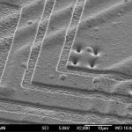
The Power of SEM Analysis
Analysis of an EEE component via a scanning electron microscope (SEM) is a truly enlightening process that may reveal things which might go undetected with less powerful equipment. By magnifying up to 250,000 times and providing a greater depth of field, a SEM can help a trained specialist uncover the telltale signs of a counterfeit part or gain insight into if and possibly why a device may have failed.
Here’s how it works. A scanning electron microscope produces images by scanning the surface with a focused beam of electrons (as opposed to light) emitted through a gun and through a series of electromagnetic lenses in the SEM column. These electrons interact with atoms in the sample, producing various signals containing information about surface and composition. The incident electron beam is scanned in a raster pattern across the surface to create an image. By synchronizing the position in the image scan to that of the scan of the incident electron beam, the display represents the surface area’s morphology.
SEM analysis is a destructive test because of the potential damage to the sample as a result of decapsulation, electron beams, and (where applicable) sputter coating. As a result, SEM analysis is generally performed only in select circumstances—and after most other tests and inspections are performed.
When to Consider SEM Analysis:
- Mandated by or assists with conformance to flowdown requirements or to an industry standard such as SAE AS6171
- Failure within the final product or system is likely result in loss of life, severe injury or major property damage
- Untraceable to OEM and supplier did not comply with AS6081 during sourcing or has recent problem reports against it
COUNTERFEIT DETECTION
Those who attempt to pass off parts as something they’re not, either as new or as a different part number, are increasingly crafty. In response more sophisticated methods are becoming increasingly essential to providing solid assurances that a part without a manufacturer’s certificate of compliance is truly new and authentic. SEM analysis is one of the best tools in the industry’s toolbox to reveal anomalies that may lead to a suspect counterfeit classification.
By inspecting the surface of a semiconductor via a SEM, surface abnormalities and modifications that might otherwise go undetected may be discovered. Zooming in closer than possible with other methods enables technicians to, for example, see contrasts between textures that may indicate a coating was applied OR identify overspills on molds as a sign that the device was blacktopped. SEM analysis can also document contrasts in laser patterns around part markings as evidence that a sample was laser etched. Surface abrasions and sanding marks may also be discovered.
FAILURE ANALYSIS
As the chips used within semiconductors become more miniaturized and complex, the causes of EC failures become more diverse and complicated. Failure analysis, for which SEM analysis can be integral, may lead to the identification of a device as the cause of failure and/or reveal the reason why a particular device failed to perform as expected. This information can be used to improve design, increase production yield, and minimize returns or repairs.
During SEM analysis, a device may be delidded and the metallization of the die inspected to search for imperfections or burn marks that might affect how a part operates. Technicians may also inspect the bonding, including where the bond attaches to the die, to confirm whether or not all the joints are clean.
At Advanced Component Testing, we can perform sophisticated SEM analysis via a Hitachi SEM. Our in-house staff can use this powerful microscope to inspect the surface for signs of adulteration during counterfeit testing or, as part of failure analysis, to check metallization and attachments for anomalies including scratches, cracks, voids and burn marks created by prior use or during the manufacturing process.


